Specializing in High Complexity PCB Design
FREEDOMCAD is is one of the largest PCB Design service providers in the US with over 30 full-time designers and engineers supporting Altium, Allegro, Xpedition, and PADS. As data rates increase, boards get denser & EMI becomes more important. The need for experienced, competent, and talented designers becomes paramount. FREEDOMCAD is here to bridge the gap, with over 800 designs completed yearly, we’ve seen it all & can support you through the entire design cycle. From creating the library footprints, mechanical outline, stack-up selection, Placement/routing, we have you covered.

HDI Stackup
Making sure there are minimal changes if any when getting feedback from your preferred Fab House. Whether you are a Cadence, Mentor or Altium user we have dedicated teams to support your requirements, utilizing the latest software with the ability to down rev to previous versions.
Design Capabilities
- Rules Driven Designs (Constraint Manager, Constraint Editor)
- Schematic and CAD Library Creation and Maintenance
- Signal & Power Integrity Analysis/Design Verification

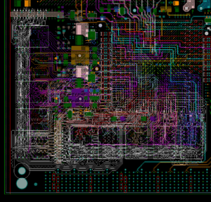
DDR4 Layout Example
- High Speed Backplane / Midplane Design
- Single Ended and Differential Controlled Impedance Design
- Design for Manufacture / Test / Assembly
- Micro BGA / Micro Via / Blind & Buried Vias
- Rigid, Flex-Rigid, and Flex Circuit Design
- Full Documentation Package Creation
- 24 X 7 Design Support
- Turnkey Hardware Services
- Remote or On-Site Design Support
Tools
Cadence Allegro
We have extensive experience with the Cadence Allegro tool suite; we currently support the latest versions of the tool. We are proud to be one of a handful of Early Adopter Program Members with Cadence.
Siemens EDA/Mentor Graphics – Xpedition
We currently support all versions of Xpedition. We have a team dedicated solely to Mentor with the experience to support projects of any complexity.
Siemens EDA/Mentor Graphics – PADS
We currently support the latest version of PADS w/ dedicated designers on staff.
Altium Designer – Official Service Bureau
We support the latest versions of Altium Designer. Our dedicated Altium designers have the experience necessary to utilize the unique features of this tool including Altium’ s powerful query engine, the new xsignal and 3D modeling capabilities.
Valor NPI Software
Valor NPI’s DFM analysis is a cornerstone process tool for Freedom CAD to assure manufacturability and minimal delays in the fabrication process. We are a Valor Certified Design Partner.
DalTools
DalTools applications integrate directly and seamlessly into Cadence Allegro tools to improve all aspects of the PCB design process.
Our Process
1. Kick-off Meeting
A Lead Designer/PM will be assigned to your project once we’ve received the Purchase Order. The kickoff meeting is an opportunity to do a full review of the project scope, discuss specific details, and answer any questions either party may have.
2. Library Development
Our dedicated Library team begins the process of creating and managing the symbols and footprints used in your PCB design. This involves creating schematic symbols, PCB footprints, and 3D models for each electronic component. If required, we can work with customer provided libraries and help manage changes.
3. Component Placement
This is the process of arranging the electronic components on the PCB in a way that meets your design requirements. The placement process considers factors such as signal integrity, power delivery, thermal management, and mechanical constraints.
4. Critical Routing
Critical routing involves routing the most important signals first. These signals include power, ground, and high-speed signals. The critical routing process ensures that these signals have the shortest and most direct paths between components.
5. Routing
Routing the traces between components is a critical step in the process and we work closely with you to ensure the routing meets your requirements. The routing process must consider factors such as signal integrity, power delivery, thermal management, and mechanical constraints.
6. Documentation
This step includes finalizing and getting customer approval on schematic diagrams, fabrication and assembly drawings & notes, title blocks, formatting, etc. to ensure that these meet your specific requirements. The documentation process ensures that the design can be easily understood and manufactured.
7. Valor/DFM Analysis
Once approved and signed-off on, all layout projects go through our standard Valor/DFM analysis utilizing the Valor NPI suite of tools. This involves analyzing the design for manufacturing issues such as board complexity, drill sizes, and tolerances. The Valor/DFM analysis process ensures that the design can be manufactured efficiently and cost-effectively.
8. Deliverables Package
FREEDOMCAD prides itself on having one of the most consistent and complete deliverables packages in the industry. Rather than have our designers generate this data, we have a dedicated Valor/DFM team that generates a standard package with all of the files required by manufacturers. This includes the board file/database itself, gerbers, ODB++, xy data, pick & place files, etc. An example dataset can be viewed here.
Contact Us to Discuss Your PCB Design or Engineering Requirements